Figure 1:Defect Evolution during Film Growth
Simulation of InGaN film growth, showing only defects.
Defect formation during semiconductor film growth defines many critical physical properties of these materials, but directly simulating atomic-scale growth dynamics has proved challenging due to complex interaction potentials and long physical timescales.
We developed a novel Stillinger–Weber potential for the InxGa1-xN system and demonstrated molecular dynamics film-growth simulations that reproduced experimentally observed defect dynamics and morphological behavior.
Approach
- Molecular dynamics vapor deposition simulations
- Novel Stillinger-Weber interatomic potential for InxGa1-xN
- Temperature and alloy composition sweeps
- Direct observation and quantitization of defect and morphology evolution
Results
Film Morphology
Our method produced stable and realistic films across multiple parameters, including alloy concentration and temperature. Pure GaN growth reproduced fine lamellar polytypism, a well-known feature of III-V systems. Higher temperatures yielded smoother, denser films, while increasing indium content promoted structural disorder, trends consistent with experimental observations.
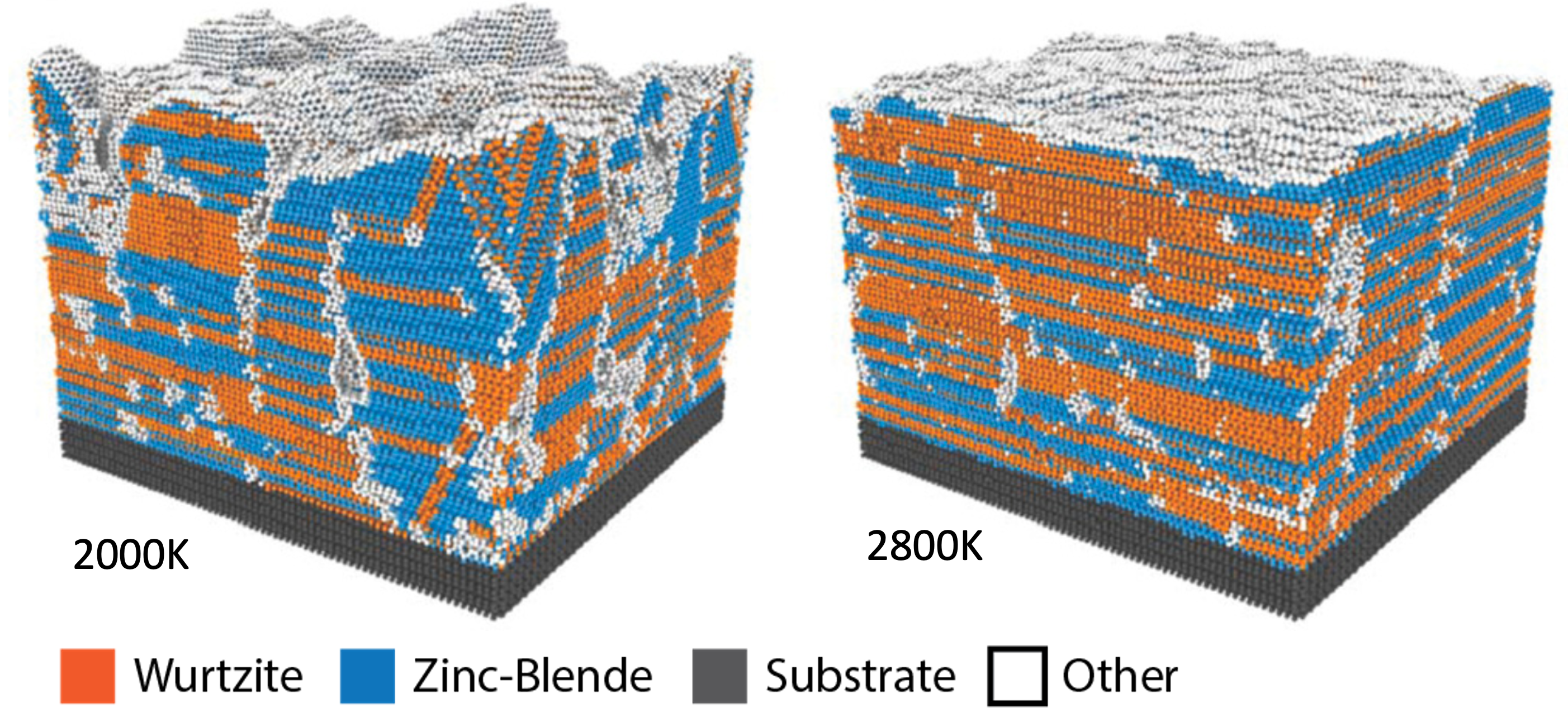
Figure 2:InN {0001} Surface Growth
Growing GaN/GaN films in the polar [0001] direction. The extremely small energy difference between the Wurtzite and Zinc-Blend structures can result in a high-degree of lamellar polytypism. The result is undesirable, but physical.
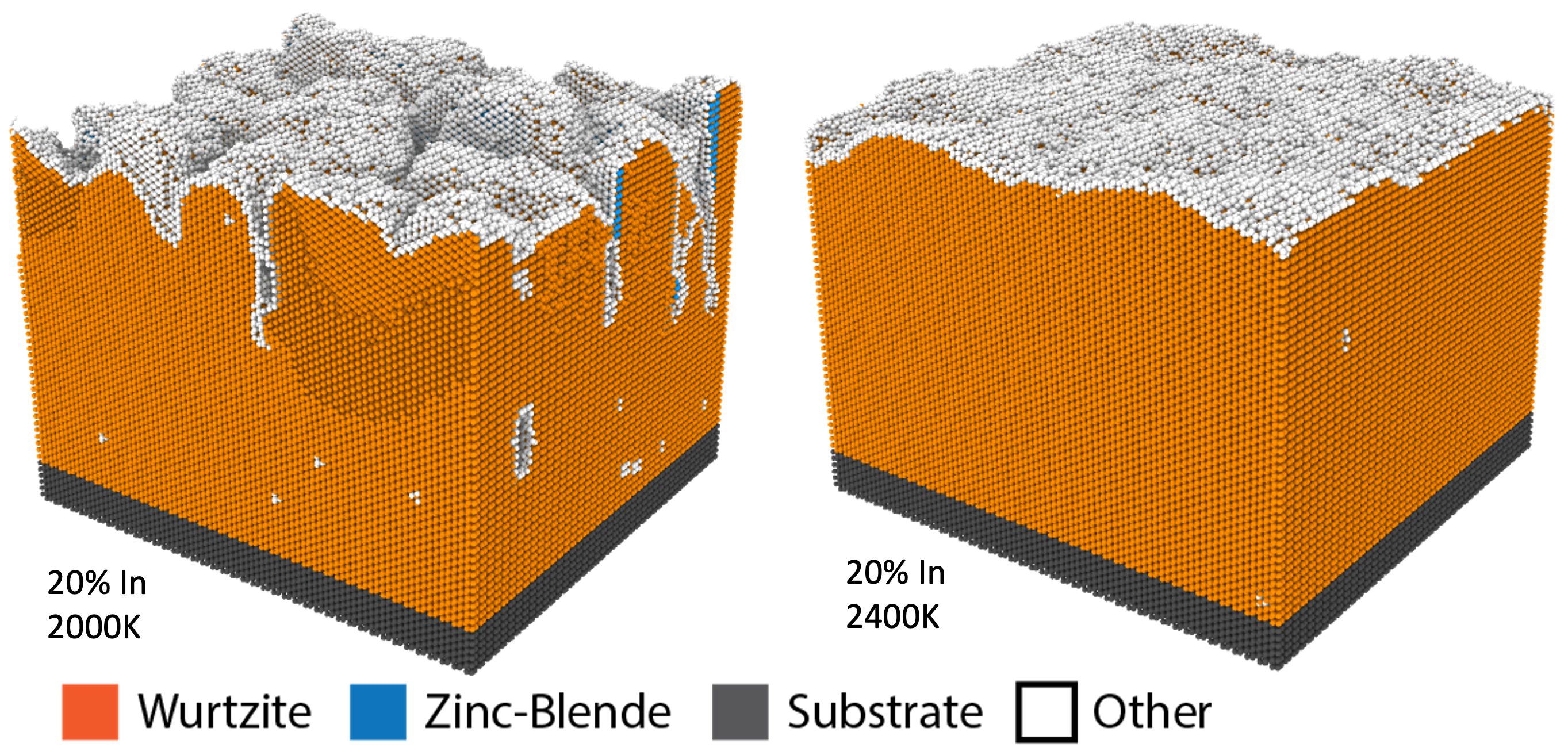
Figure 3:In0.8Ga0.2N Growth
Growth of the In0.8Ga0.2 alloy. The bonding asymmetry induced by alloying elimates polytypism.
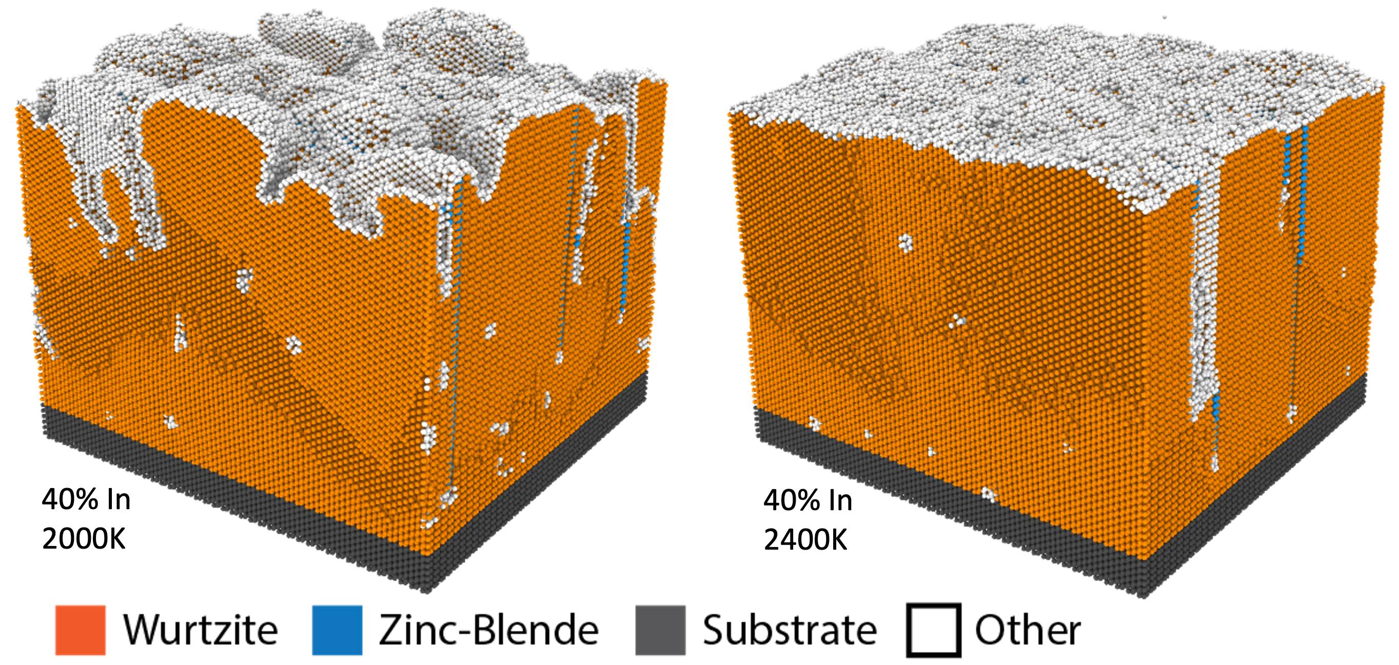
Figure 4:In0.6Ga0.4N Growth
In0.6Ga0.4N film structures are more disordered. Vertical blue lines represent threading dislocations, while white clusters represent vacancies or the termination of misfit dislocations near the substrate.
Point Defects
Calculation of defect concentrations revealed a distinction between growth defects that decrease with temperature, and thermal defects that increase with temperature.
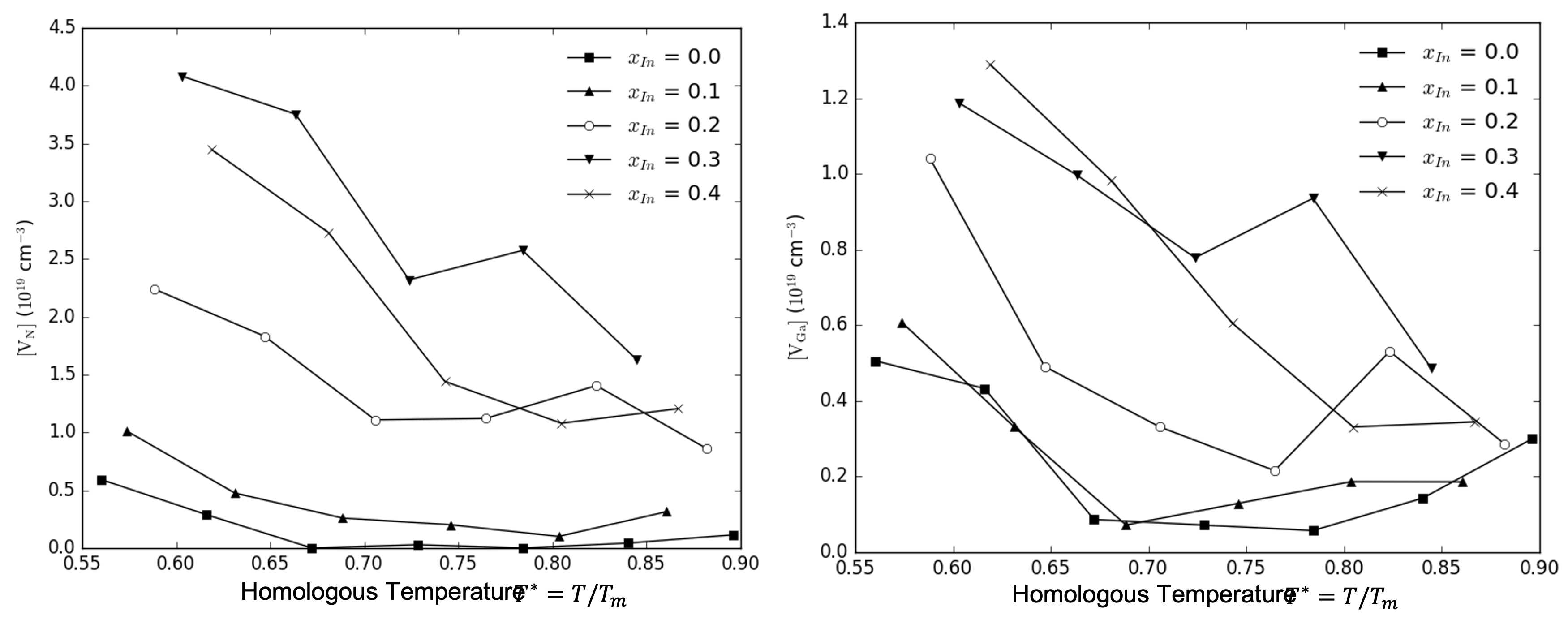
Figure 5:Vacancy Concentration
(left) Nitrogren vacancies decrease with temperature in all cases, suggesting these are mostly unstable growth defects even near the melting temperature. (right) Gallium-site vacancies show a more pronounced uptick at high temperatures, especially for low indium content, suggesting thermal vacancies and a natural tendency to become gallium deficient at high temperature.
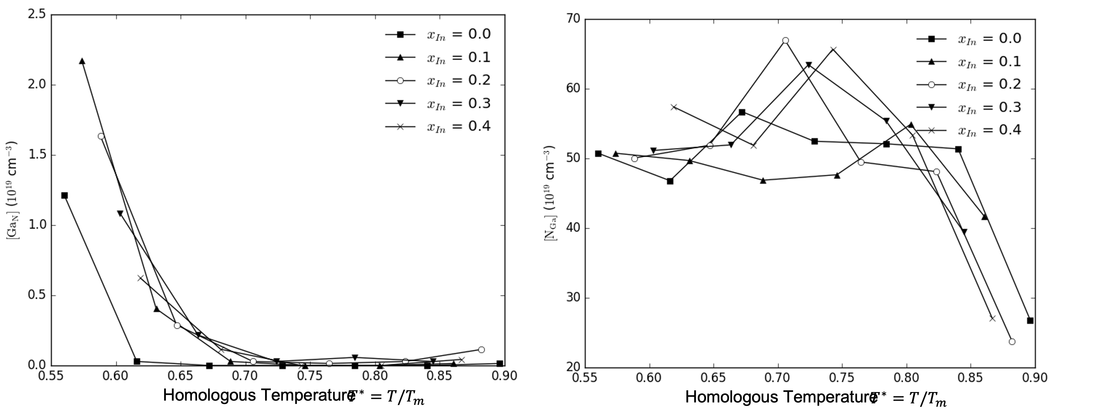
Figure 6:Antisite Concentration
(left) Gallium-on-nitrogen occurs at low temperature, but drops off steeply. (right) Nitrogen-on-gallium occur relative consistently up until high temperature. This suggests kinetic limiting of nitrogen atoms at most growth temperatures.
Dislocations
We identified dislocations using the DXA algorithm. Vertical threading and horizontal misfit both appeared. While we were not able to grow epitaxial films on this first attempt, both types of dislocations showed reasonable behavior, including the migration of misfit dislocation from the surface to the interface during growth.
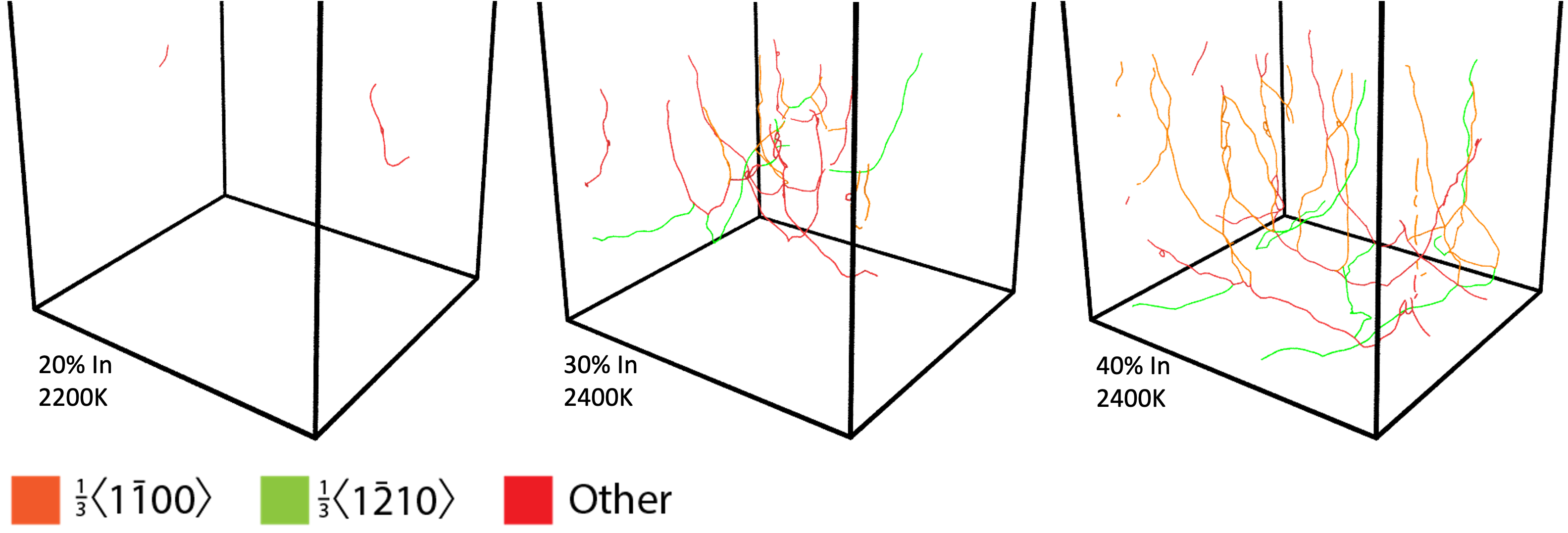
Figure 7:Dislocation Network Visualization
Dislocation concentration explodes past 20% indium content. Vertical dislocations are threading dislocations (mostly orange), while horizontal dislocation near the substrate are misfit dislocations (mostly green/red)
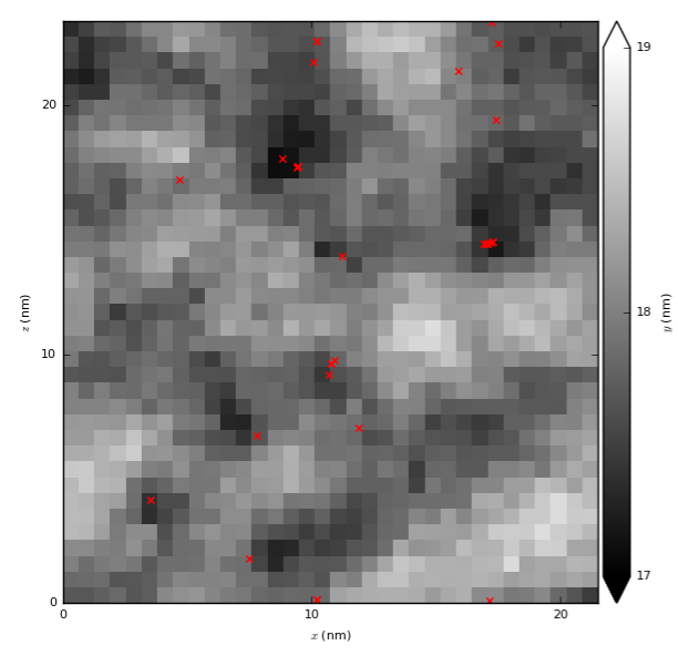
Figure 8:Threading Dislocations
Threading dislocations overlayed on a map of the film's surface height. Threading dislocations exit at pits.
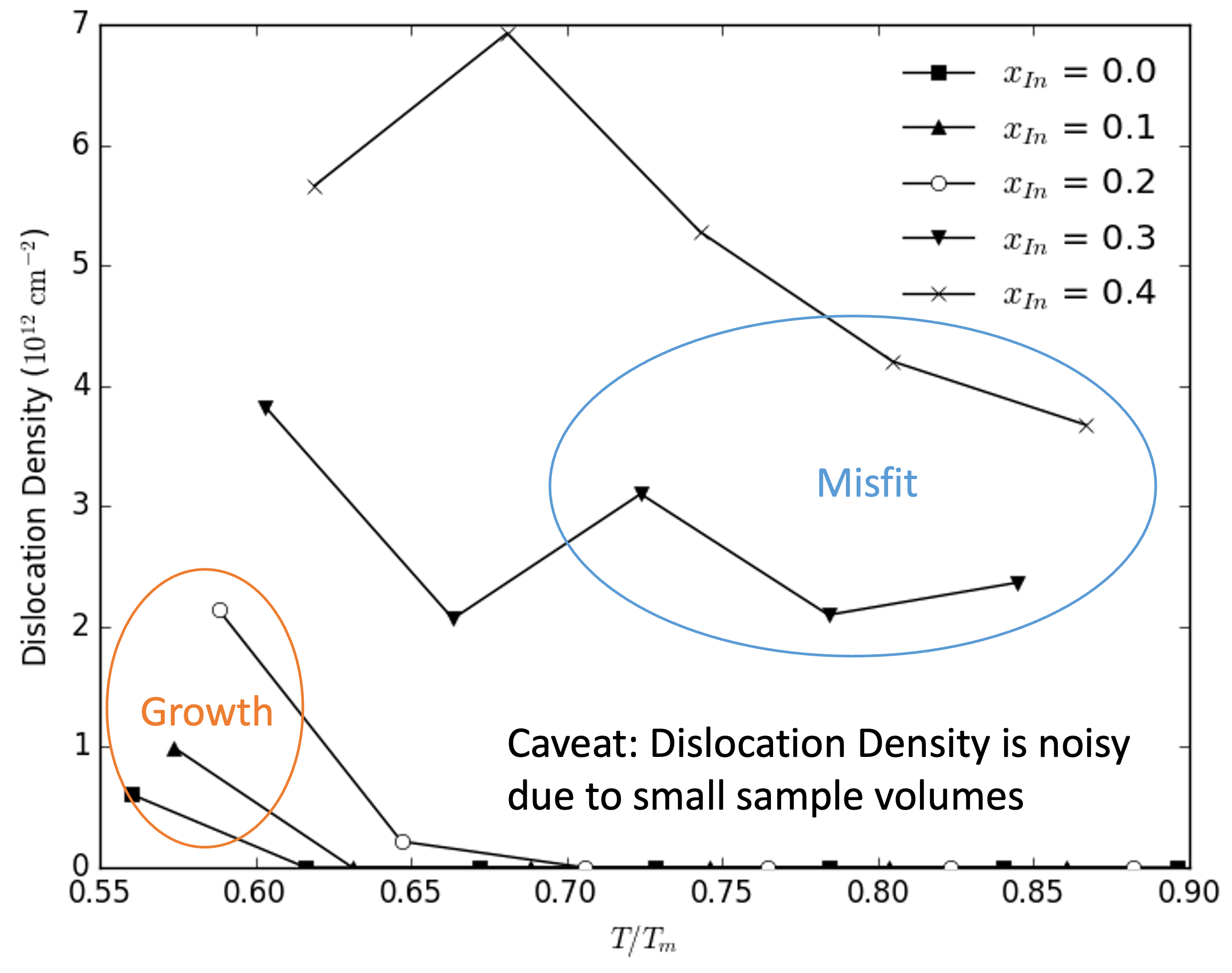
Figure 9:Dislocation Concentration
Dislocation contration for various film compositions and temperatures. Threading dislocations and other growth dislocation disappear as temperature increased. Misfit dislocations, caused by high indium content, remain even at high temperatures.
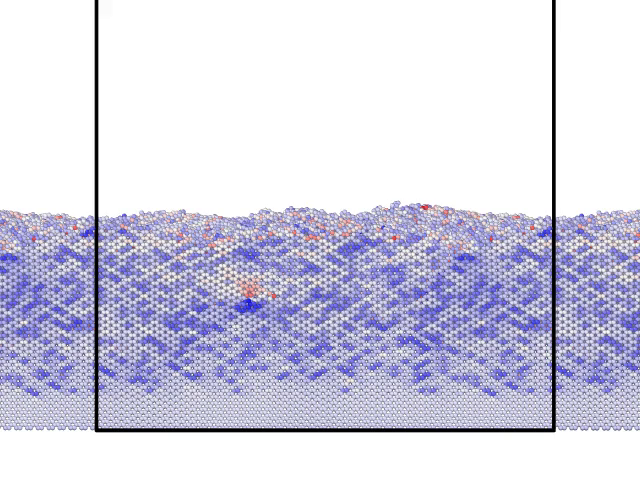
Figure 10:Misfit Dislocation Migration
Misfit strain relaxation by dislocation migration to the film/substrate interface.
Conclusion
These simulations demonstrate that molecular dynamics can reproduce several experimentally observed features of semiconductor film growth, especially the realistic morphology evolution and defect formation. Despite limited spatial and temporal scale, the atomistic simulation approach captured physically meaningful trends across alloy composition and temperature. Carefully parameterized molecular dynamics can serve as a useful exploratory tool for studying nonequilibrium growth processes in complex semiconductor systems.
Further Reading
Molecular dynamics studies of InGaN growth on nonpolar (110) GaN surfaces
K. Chu, J. Gruber, X.W. Zhou, R.E. Jones, S.R. Lee, G.J. Tucker
Physical Review Materials
(2018)
[link]
Molecular dynamics simulations of substitutional diffusion
X.W. Zhou, R.E. Jones, J. Gruber
Computational Materials Science
(2017)
[link]
Molecular dynamics studies of defect formation during heteroepitaxial growth of InGaN alloys on (0001) GaN surfaces
J. Gruber, X.W. Zhou, R.E. Jones, S.R. Lee, G.J. Tucker
J Appl Phys
(2017)
[link]